- 您现在的位置:买卖IC网 > Sheet目录487 > NTD4965NT4G (ON Semiconductor)MOSFET N-CH 30V 68A DPAK
�� �
�
�NTD4965N�
�Power� MOSFET�
�30� V,� 68� A,� Single� N� ?� Channel,� DPAK/IPAK�
�Features�
�?� Low� R� DS(on)� to� Minimize� Conduction� Losses�
�?� Low� Capacitance� to� Minimize� Driver� Losses�
�?� Optimized� Gate� Charge� to� Minimize� Switching� Losses�
�?� Three� Package� Variations� for� Design� Flexibility�
�?� These� Devices� are� Pb� ?� Free,� Halogen� Free/BFR� Free� and� are� RoHS�
�Compliant�
�Applications�
�?� CPU� Power� Delivery�
�?� DC� ?� DC� Converters�
�V� (BR)DSS�
�30� V�
�http://onsemi.com�
�R� DS(ON)� MAX�
�4.7� m� W� @� 10� V�
�10� m� W� @� 4.5� V�
�D�
�I� D� MAX�
�68� A�
�MAXIMUM� RATINGS� (T� J� =� 25� °� C� unless� otherwise� stated)�
�Parameter�
�Drain� ?� to� ?� Source� Voltage�
�Symbol�
�V� DSS�
�Value�
�30�
�Unit�
�V�
�G�
�Gate� ?� to� ?� Source� Voltage�
�Continuous� Drain�
�Current� R� q� JA�
�(Note� 1)�
�T� A� =� 25� °� C�
�T� A� =� 100� °� C�
�V� GS�
�I� D�
�±� 20�
�17.8�
�12.6�
�V�
�A�
�S�
�N� ?� CHANNEL� MOSFET�
�Power�
�Dissipation� R� q� JA�
�(Note� 1)�
�T� A� =� 25� °� C�
�P� D�
�2.6�
�W�
�4�
�4�
�4�
�1�
�2� 3�
�3�
�Continuous� Drain�
�Current� R� q� JA�
�(Note� 2)�
�Power�
�Dissipation� R� q� JA�
�(Note� 2)�
�Continuous� Drain�
�Current� R� q� JC�
�(Note� 1)�
�Steady�
�State�
�T� A� =� 25� °� C�
�T� A� =� 100� °� C�
�T� A� =� 25� °� C�
�T� C� =� 25� °� C�
�T� C� =� 100� °� C�
�I� D�
�P� D�
�I� D�
�13.0�
�9.2�
�1.39�
�68�
�48�
�A�
�W�
�A�
�1� 2�
�3�
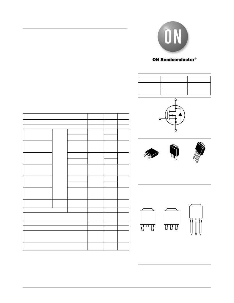
�CASE� 369AA�
�DPAK�
�(Bent� Lead)�
�STYLE� 2�
�1�
�2�
�CASE� 369AC� CASE� 369D�
�3� IPAK� IPAK�
�(Straight� Lead)� (Straight� Lead�
�DPAK)�
�4�
�Power�
�Dissipation� R� q� JC�
�(Note� 1)�
�Pulsed� Drain� t� p� =10� m� s�
�Current�
�Current� Limited� by� Package�
�T� C� =� 25� °� C�
�T� A� =� 25� °� C�
�T� A� =� 25� °� C�
�P� D�
�I� DM�
�I� DmaxPkg�
�38.5�
�248�
�76�
�W�
�A�
�A�
�4�
�Drain�
�MARKING� DIAGRAMS�
�&� PIN� ASSIGNMENTS�
�4�
�Drain�
�Drain�
�Operating� Junction� and� Storage�
�Temperature�
�Source� Current� (Body� Diode)�
�T� J� ,�
�T� STG�
�I� S�
�?� 55� to�
�+175�
�35�
�°� C�
�A�
�1�
�2�
�3�
�Source� Gate� Drain� Source�
�1�
�2�
�3�
�Drain� to� Source� dV/dt�
�Single� Pulse� Drain� ?� to� ?� Source� Avalanche�
�Energy� (T� J� =� 25� °� C,� V� DD� =� 24� V,� V� GS� =� 10� V,�
�I� L� =� 31� A� pk� ,� L� =� 0.1� mH,� R� G� =� 25� W)�
�dV/dt�
�EAS�
�6.0�
�47�
�V/ns�
�mJ�
�2�
�1� Drain� 3�
�Gate�
�Gate� Drain� Source�
�Lead� Temperature� for� Soldering� Purposes�
�(1/8”� from� case� for� 10� s)�
�T� L�
�260�
�°� C�
�Y�
�=� Year�
�Stresses� exceeding� Maximum� Ratings� may� damage� the� device.� Maximum�
�Ratings� are� stress� ratings� only.� Functional� operation� above� the� Recommended�
�Operating� Conditions� is� not� implied.� Extended� exposure� to� stresses� above� the�
�Recommended� Operating� Conditions� may� affect� device� reliability.�
�1.� Surface� ?� mounted� on� FR4� board� using� 1� sq� ?� in� pad,� 1� oz� Cu.�
�2.� Surface� ?� mounted� on� FR4� board� using� the� minimum� recommended� pad� size.�
�WW� =� Work� Week�
�4965N� =� Device� Code�
�G� =� Pb� ?� Free� Package�
�ORDERING� INFORMATION�
�See� detailed� ordering� and� shipping� information� in� the� package�
�dimensions� section� on� page� 3� of� this� data� sheet.�
�?� Semiconductor� Components� Industries,� LLC,� 2012�
�August,� 2012� ?� Rev.� 2�
�1�
�Publication� Order� Number:�
�NTD4965N/D�
�发布紧急采购,3分钟左右您将得到回复。
相关PDF资料
NTD4970N-35G
MOSFET N-CH 30V 38A IPAK
NTD50N03RT4G
MOSFET N-CH 25V 7.8A DPAK
NTD5413NT4G
MOSFET N-CH 60V 30A DPAK
NTD5414NT4G
MOSFET N-CH 60V 24A DPAK
NTD5802NT4G
MOSFET N-CH 40V 16.4A DPAK
NTD5803NT4G
MOSFET N-CH 40V 76A DPAK
NTD5804NT4G
MOSFET N-CH 40V 69A DPAK
NTD5805NT4G
MOSFET N-CH 40V 51A DPAK
相关代理商/技术参数
NTD4969N
制造商:ONSEMI 制造商全称:ON Semiconductor 功能描述:Power MOSFET 30 V, 41 A, Single N?Channel, DPAK/IPAK CPU Power Delivery
NTD4969N-1G
功能描述:MOSFET TRENCH 3.1 30V 9 mOhm NCH RoHS:否 制造商:STMicroelectronics 晶体管极性:N-Channel 汲极/源极击穿电压:650 V 闸/源击穿电压:25 V 漏极连续电流:130 A 电阻汲极/源极 RDS(导通):0.014 Ohms 配置:Single 最大工作温度: 安装风格:Through Hole 封装 / 箱体:Max247 封装:Tube
NTD4969N-35G
功能描述:MOSFET TRENCH 3.1 30V 9 mOhm NCH RoHS:否 制造商:STMicroelectronics 晶体管极性:N-Channel 汲极/源极击穿电压:650 V 闸/源击穿电压:25 V 漏极连续电流:130 A 电阻汲极/源极 RDS(导通):0.014 Ohms 配置:Single 最大工作温度: 安装风格:Through Hole 封装 / 箱体:Max247 封装:Tube
NTD4969NT4G
功能描述:MOSFET TRENCH 3.1 30V 9 mOhm NCH RoHS:否 制造商:STMicroelectronics 晶体管极性:N-Channel 汲极/源极击穿电压:650 V 闸/源击穿电压:25 V 漏极连续电流:130 A 电阻汲极/源极 RDS(导通):0.014 Ohms 配置:Single 最大工作温度: 安装风格:Through Hole 封装 / 箱体:Max247 封装:Tube
NTD4970N
制造商:ONSEMI 制造商全称:ON Semiconductor 功能描述:Power MOSFET 30 V, 36 A, Single Na??Channel, DPAK/IPAK
NTD4970N-1G
功能描述:MOSFET NFET DPAK 30V 38A 11MOHM RoHS:否 制造商:STMicroelectronics 晶体管极性:N-Channel 汲极/源极击穿电压:650 V 闸/源击穿电压:25 V 漏极连续电流:130 A 电阻汲极/源极 RDS(导通):0.014 Ohms 配置:Single 最大工作温度: 安装风格:Through Hole 封装 / 箱体:Max247 封装:Tube
NTD4970N-35G
功能描述:MOSFET NFET DPAK 30V 38A 11MOHM RoHS:否 制造商:STMicroelectronics 晶体管极性:N-Channel 汲极/源极击穿电压:650 V 闸/源击穿电压:25 V 漏极连续电流:130 A 电阻汲极/源极 RDS(导通):0.014 Ohms 配置:Single 最大工作温度: 安装风格:Through Hole 封装 / 箱体:Max247 封装:Tube
NTD4970NT4G
功能描述:MOSFET NFET DPAK 30V 38A 11MOHM RoHS:否 制造商:STMicroelectronics 晶体管极性:N-Channel 汲极/源极击穿电压:650 V 闸/源击穿电压:25 V 漏极连续电流:130 A 电阻汲极/源极 RDS(导通):0.014 Ohms 配置:Single 最大工作温度: 安装风格:Through Hole 封装 / 箱体:Max247 封装:Tube